
-
1. A-002-001-001: What two elements widely used in semiconductor devices exhibit both metallic and non-metallic characteristics?
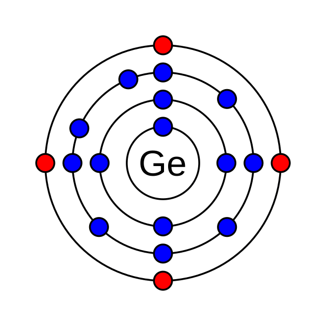
Silicon and Germanium: Dual-Natured Conductors (A-002-001-001)
Silicon and Germanium: Semiconductors at the Core:
Question A-002-001-001 examines the two elements widely used in semiconductor devices for their metallic and non-metallic characteristics. The correct answer, B) Silicon and germanium, spotlights their fundamental role in semiconductor technology. Silicon and germanium are prized for their ability to conduct electricity under certain conditions and act as insulators in others. This dual-natured behavior is the cornerstone of modern electronics, allowing for the creation of devices like transistors and diodes that can control and manipulate electrical currents. In ham radio, these materials are integral to the components that make up receivers, transmitters, and other essential equipment, playing a crucial role in signal processing, amplification, and frequency modulation.Understanding the properties and applications of silicon and germanium is not just fundamental for those interested in the technical aspects of ham radio but also for anyone involved in electronics. Their versatility and the ability to alter their conductive properties through doping make them indispensable in a wide range of applications, driving innovation and functionality in the field of electronics.
Parallels:
- Chameleons of the Material World: Just as chameleons change their color to adapt to different environments, silicon and germanium can exhibit both conductive and insulative properties, adapting to the needs of electronic circuits and making them versatile and essential materials in the field.
- The Jekyll and Hyde of Elements: Silicon and germanium are like the literary characters Dr. Jekyll and Mr. Hyde, possessing two distinct ‘personalities’—one conductive and one insulative. This duality is harnessed in semiconductors to switch between conducting and insulating states, enabling the complex operations of electronic devices.
Question Summary and Key Takeaways:
- Dual Characteristics: Silicon and germanium exhibit both metallic and non-metallic characteristics, making them versatile for various semiconductor applications.
- Fundamental in Electronics: Their ability to alter conductive properties is fundamental to creating components like diodes and transistors.
- Ham Radio Applications: These materials are crucial in the manufacturing of components that make up essential ham radio equipment.
- Versatility through Doping: The process of doping allows for the manipulation of their conductive properties, enhancing their functionality in electronic devices.
- Understanding for Innovation: A deep understanding of these materials and their properties is essential for innovation and advancement in electronics and ham radio technology.
-
2. A-002-001-002: In what application is gallium-arsenide used as a semiconductor material in preference to germanium or silicon?
Gallium Arsenide: The High-Frequency Choice (A-002-001-002)
Gallium Arsenide: Superior Performance at Microwaves:
Question A-002-001-002 inquires about the preferred application of gallium-arsenide as a semiconductor material. The correct answer, B) At microwave frequencies, highlights its significance in high-frequency applications. Gallium arsenide is favored over silicon and germanium in these scenarios due to its superior electron mobility, allowing for faster signal processing and less noise, which is critical at microwave frequencies. This makes it an ideal material for components in advanced communication systems, including satellite communication and radar, and in ham radio systems for high-frequency operations. Its usage represents a step forward in achieving greater efficiency and performance in devices operating at these higher frequencies.The choice of gallium arsenide in specific applications underscores the importance of selecting the right material based on the operational requirements. In ham radio, understanding when to use gallium arsenide can significantly impact the performance and capabilities of the system, particularly in activities that require precise and efficient high-frequency operations.
Parallels:
- High-Speed Trains for Rapid Transit: Just as high-speed trains are chosen for quick transit over long distances, gallium arsenide is chosen for high-frequency applications where speed and performance are paramount.
- The Sprinter in a Relay Race: Consider gallium arsenide as the sprinter in a relay race, where speed and efficiency are crucial. In electronic circuits, it’s the material that ‘sprints’ to ensure rapid and efficient signal processing at microwave frequencies.
Question Summary and Key Takeaways:
- Microwave Frequency Applications: Gallium arsenide is preferred for its superior performance in high-frequency, particularly microwave, applications.
- Superior Electron Mobility: Its high electron mobility allows for faster signal processing and reduced noise, essential for advanced communication systems.
- Strategic Material Choice: Understanding the operational requirements and choosing the appropriate semiconductor material, like gallium arsenide, can significantly impact system performance.
- Ham Radio Advancement: Incorporating gallium arsenide in ham radio systems can enhance capabilities, especially in high-frequency operations.
- Material Innovation: The development and application of materials like gallium arsenide drive innovation and performance in the electronics field.
-
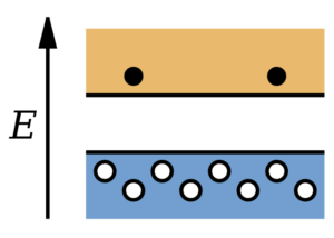
3. A-002-001-003: What type of semiconductor material contains fewer free electrons than pure germanium or silicon crystals?
P-Type Semiconductors: The Positive Side (A-002-001-003)
P-Type Semiconductors: Fewer Electrons, More Holes:
Question A-002-001-003 explores the type of semiconductor material that contains fewer free electrons than pure germanium or silicon crystals. The correct answer, B) P-type, delineates a fundamental category in semiconductor technology. P-type semiconductors are created by doping pure silicon or germanium with elements that have fewer valence electrons, resulting in the creation of ‘holes’ or positive charge carriers. These holes play a critical role in the conduction process, moving throughout the material and allowing for the flow of current. In ham radio components, such as transistors and diodes, the interaction between P-type and N-type materials is fundamental to their operation, enabling the control and amplification of signals.Understanding the behavior of P-type semiconductors is crucial not just for the construction and repair of electronic components but also for the innovation and advancement of semiconductor technology. The ability to manipulate the electrical properties of materials like silicon and germanium by introducing different impurities is what allows for the wide array of electronic devices we rely on today.
Parallels:
- The Balloon with Missing Air: Just as a balloon with less air has room to take in more, P-type semiconductors with fewer electrons have ‘holes’ that allow for the movement of charge, essential for the flow of current in electronic devices.
- A Puzzle Missing Pieces: Consider P-type semiconductors like a puzzle with missing pieces. The ‘holes’ left by absent electrons are like the spaces waiting to be filled, and when they are, it allows for the complete picture—or current flow—to emerge.
Question Summary and Key Takeaways:
- Hole Conduction: P-type semiconductors contain fewer free electrons and more ‘holes’, acting as positive charge carriers.
- Doping Process: The creation of P-type materials involves doping with elements that have fewer valence electrons than silicon or germanium.
- Critical in Components: P-type materials are fundamental in the operation of various electronic components used in ham radio, such as transistors and diodes.
- Understanding for Innovation: Knowledge of how P-type semiconductors function is crucial for anyone involved in designing, building, or repairing electronic devices.
- Electrical Property Manipulation: The ability to alter the electrical properties of materials through doping is a cornerstone of semiconductor technology and electronic innovation.

-
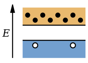
4. A-002-001-004: What type of semiconductor material contains more free electrons than pure germanium or silicon crystals?
N-Type Semiconductors: The Negative Charge Carriers (A-002-001-004)
N-Type Semiconductors: Abundance of Free Electrons:
Question A-002-001-004 asks about the type of semiconductor material that contains more free electrons than pure germanium or silicon crystals. The correct answer, C) N-type, highlights the characteristics of N-type semiconductors, which are doped with elements that have an extra valence electron, resulting in an abundance of free electrons. These free electrons act as the primary charge carriers, making N-type materials crucial for conducting electricity in electronic devices. In ham radio systems, N-type semiconductors are often used in conjunction with P-type materials to form p-n junctions, the fundamental building blocks of diodes and transistors that control and amplify signals.Understanding the behavior and role of N-type semiconductors is essential for anyone involved in electronics and ham radio. Their ability to efficiently conduct electrical current underpins the functionality of a vast array of devices and systems, making them a key component in the world of semiconductor technology.
Parallels:
- River of Electrons: Think of N-type semiconductors as a river with a strong current. The free electrons are like the water molecules flowing rapidly, carrying energy and momentum, essential for conducting electricity through the material.
- The Busy Highway: Envision a busy highway filled with cars (free electrons) moving swiftly towards their destination. N-type semiconductors provide a similar ‘highway’ for electrons to travel, facilitating the fast and efficient flow of electrical current.
Question Summary and Key Takeaways:
- Abundance of Electrons: N-type semiconductors are characterized by their surplus of free electrons, serving as negative charge carriers.
- Doping Process: They are created by doping silicon or germanium with elements that provide an extra valence electron.
- Essential for Device Operation: N-type materials are fundamental in the construction of diodes, transistors, and other electronic components in ham radio equipment.
- Conductivity and Functionality: The free electrons in N-type semiconductors are crucial for the efficient conduction of electricity and the overall functionality of electronic devices.
- Understanding for Advancement: Comprehending the properties and applications of N-type semiconductors is vital for the advancement and innovation in electronics and ham radio technology.
-
5. A-002-001-005: What are the majority charge carriers in P-type semiconductor material?
P-Type Semiconductors: Understanding Majority Charge Carriers (A-002-001-005)
P-Type Semiconductors: Dominance of Holes:
Question A-002-001-005 explores the majority charge carriers in P-type semiconductor material. The correct answer, C) Holes, sheds light on the unique conduction mechanism in P-type materials. In these semiconductors, ‘holes’ or the absence of electrons, act as the majority charge carriers. When an electron moves to fill a hole, it leaves behind a new hole, effectively allowing the holes to move through the material and conduct electricity. This movement of positive charge carriers is fundamental to the operation of various electronic components, including those used in ham radio systems, where P-type materials are often paired with N-type materials to form devices that control and modulate signals.Understanding the concept of holes and how they contribute to electrical conduction is crucial for anyone delving into electronics and ham radio technology. The behavior of these charge carriers underpins many of the functionalities we rely on in modern electronic devices.
Parallels:
- The Dance Floor Shuffle: Imagine a crowded dance floor where dancers (electrons) move to fill empty spaces (holes). As one dancer moves, they leave behind a new space, creating a continuous flow of movement. Similarly, in P-type semiconductors, the movement of holes facilitates the flow of electrical charge.
- Musical Chairs: Consider the game of musical chairs, where participants (electrons) move to occupy empty chairs (holes) when the music stops. Each time a participant fills a chair, a new empty chair is created elsewhere. This is akin to how holes in P-type materials move and carry charge.
Question Summary and Key Takeaways:
- Holes as Charge Carriers: In P-type semiconductors, ‘holes’ act as the majority charge carriers, playing a crucial role in electrical conduction.
- Conduction Mechanism: The movement of holes, essentially the absence of electrons, facilitates the flow of positive charge through the material.
- Component Functionality: Understanding the behavior of holes is essential for grasping the functionality of various electronic components in ham radio systems.
- Pairing with N-Type: P-type materials are often used alongside N-type materials in electronic devices, forming p-n junctions crucial for signal control and modulation.
- Electrical Understanding: Comprehending the role and movement of holes in P-type semiconductors enhances one’s ability to innovate and troubleshoot in the field of electronics and ham radio.
-
6. A-002-001-006: What are the majority charge carriers in N-type semiconductor material?
N-Type Semiconductors: Identifying Majority Charge Carriers (A-002-001-006)
N-Type Semiconductors: A Sea of Free Electrons:
Question A-002-001-006 seeks to identify the majority charge carriers in N-type semiconductor material. The correct answer, C) Free electrons, emphasizes the defining characteristic of N-type materials. In these semiconductors, the doping process introduces extra electrons, making free electrons the majority charge carriers. These negatively charged particles are responsible for conducting electricity through the material, facilitating the operation of a wide range of electronic devices, including those integral to ham radio technology. The efficient movement of these electrons through N-type materials is crucial for the functionality of diodes, transistors, and other components that control, amplify, and process signals.Understanding the role of free electrons in N-type semiconductors is fundamental for anyone involved in the design, construction, or maintenance of electronic systems. Their ability to carry charge efficiently makes them a key element in the world of semiconductor technology.
Parallels:
- River Currents Carrying Leaves: Envision a river where the current (electrical field) carries leaves (free electrons) downstream. In N-type semiconductors, free electrons move through the material like leaves carried by a river, facilitating the flow of electrical charge.
- The Wind in a Field of Wheat: Think of a strong wind moving through a wheat field, causing the stalks (electrons) to sway and move in unison. Similarly, in N-type materials, an electrical field causes the free electrons to move together, creating a current and conducting electricity.
Question Summary and Key Takeaways:
- Free Electrons as Majority Carriers: In N-type semiconductors, free electrons are the majority charge carriers, essential for conducting electricity.
- Fundamental to Device Operation: The movement of these electrons is fundamental to the operation of various electronic devices, including those used in ham radio.
- Efficient Charge Carriers: Free electrons in N-type materials move efficiently, contributing to the functionality and performance of electronic components.
- Doping Process Impact: The doping process that introduces extra electrons is key to creating the N-type characteristics.
- Technical Insight: A thorough understanding of free electrons’ role in N-type semiconductors is crucial for those engaged in electronics and ham radio technology.
-
7. A-002-001-007: Silicon in its pure form is:
Silicon’s Surprising Nature: Insulator or Semiconductor? (A-002-001-007)
Silicon’s Dual Identity in Electronics:
Question A-002-001-007 addresses the nature of silicon in its purest form. The correct answer, C) an insulator, might come as a surprise given silicon’s widespread use as a semiconductor. Pure silicon lacks free charge carriers, making it an excellent insulator. However, when doped with specific impurities, its character shifts, allowing it to conduct electricity under certain conditions. This transformative ability is what makes silicon the backbone of the semiconductor industry, including its pivotal role in ham radio technology. Devices like diodes, transistors, and integrated circuits all rely on silicon’s ability to switch between conducting and insulating states, enabling the complex functions needed for communication and signal processing.Understanding silicon’s insulating properties in its pure state is crucial. It underscores the significance of the doping process that introduces controlled impurities to modify its electrical characteristics, turning an otherwise insulating material into a versatile and efficient semiconductor.
Parallels:
- Blank Canvas to Masterpiece: Just as a blank canvas can be transformed into a masterpiece with the artist’s strokes, pure silicon can be transformed into a functional semiconductor with the precise addition of impurities.
- The Chameleon of Materials: Consider silicon as a chameleon capable of changing its ‘color’—from an insulator to a semiconductor. This adaptability, much like a chameleon’s ability to change its appearance, is what makes silicon so valuable in electronics.
Question Summary and Key Takeaways:
- Insulating Nature: In its pure state, silicon acts as an insulator, lacking free charge carriers to conduct electricity.
- Transformation through Doping: The addition of impurities transforms silicon into a semiconductor, enabling its widespread use in electronic devices.
- Backbone of Electronics: Silicon’s ability to switch between conducting and insulating states is fundamental to the semiconductor industry and ham radio technology.
- Significance of Purity: Understanding the insulating nature of pure silicon highlights the importance of the doping process in semiconductor manufacturing.
- Material Versatility: Silicon exemplifies material versatility, serving as the foundation for a multitude of electronic components and systems.
-
8. A-002-001-008: An element which is sometimes an insulator and sometimes a conductor is called a:
Semiconductors: Between Conductors and Insulators (A-002-001-008)
Semiconductors: The Middle Ground of Electrical Conductivity:
Question A-002-001-008 seeks to define a material that can act as both an insulator and a conductor. The correct answer, B) semiconductor, captures the essence of materials like silicon and germanium when doped appropriately. Semiconductors are the linchpin of modern electronics, including ham radio devices, because of their ability to control the flow of electrical current. This control is achieved by manipulating their conductive properties through doping, which adds impurities to an otherwise insulating material, creating conditions where it can conduct electricity under certain circumstances. This unique position between conductors and insulators makes semiconductors indispensable in creating components that can switch, amplify, and modulate signals.The behavior of semiconductors is at the heart of electronic innovation, enabling the complex functionalities required in today’s technology. Understanding how semiconductors bridge the gap between conductors and insulators provides a fundamental insight into the workings of a vast array of electronic devices and systems.
Parallels:
- The Bilingual Communicator: Imagine a person who can speak two languages, bridging communication gaps between different groups. Semiconductors act similarly, bridging the gap between conductors and insulators, facilitating the flow of electricity in a controlled manner.
- Thermostat in a Home: A thermostat regulates a home’s temperature, maintaining a comfortable middle ground. Semiconductors regulate the flow of electrical current, maintaining a balance between conducting and insulating, essential for the functionality of electronic devices.
Question Summary and Key Takeaways:
- Bridging Conductors and Insulators: Semiconductors fill the gap between conductors and insulators, offering controlled electrical conductivity.
- Fundamental to Electronics: Their unique properties make semiconductors fundamental to the operation of almost all modern electronic devices.
- Doping is Key: The process of doping is crucial in altering an insulating material’s properties to make it conductive under certain conditions.
- Versatile Applications: Semiconductors are used in a wide range of applications, from simple diodes to complex integrated circuits.
- Understanding for Innovation: A solid grasp of semiconductor properties and behavior is essential for innovation and advancement in electronics and ham radio technology.
-
9. A-002-001-009: Which of the following materials is used to make a semiconductor?
Silicon: The Semiconductor Standard (A-002-001-009)
Silicon: The Cornerstone of Semiconductor Devices:
Question A-002-001-009 asks which material is commonly used to make semiconductors. The correct answer, D) Silicon, emphasizes its dominant role in the semiconductor industry. Silicon’s physical and chemical properties make it ideally suited for controlling electrical currents in a wide range of devices. Its abundance and cost-effectiveness further solidify its status as the material of choice for the majority of semiconductor applications, including those in ham radio technology. Devices such as diodes, transistors, and integrated circuits all rely on silicon’s semiconducting properties to perform functions like signal amplification, frequency modulation, and power regulation.Silicon’s role in semiconductor manufacturing is akin to a foundational building block in construction. It provides the base upon which the complexities of electronic circuitry are built, driving the functionality and innovation in the field.
Parallels:
- The Foundation of a Skyscraper: Just as a strong foundation is critical for building a towering skyscraper, silicon provides the fundamental base for constructing a wide array of semiconductor devices, supporting the complex structures of modern electronics.
- The Main Ingredient in a Recipe: Consider silicon as the flour in a cake recipe—essential and foundational. Without it, the end product wouldn’t hold together. Similarly, without silicon, many semiconductor devices would not be feasible.
Question Summary and Key Takeaways:
- Primary Material: Silicon is the primary material used in the manufacturing of semiconductors due to its ideal properties and abundance.
- Pervasive in Electronics: Its use is widespread across various electronic components and systems, including those in ham radio technology.
- Base for Innovation: Silicon serves as the foundational material upon which the complexities of electronic devices are built.
- Cost-Effective: Its abundance and cost-effectiveness make it a practical choice for a wide range of applications.
- Crucial Understanding: Knowledge of silicon’s role and properties is crucial for anyone involved in electronics and semiconductor technology.
-
10. A-002-001-010: Substances such as silicon in a pure state are usually good:
Pure Silicon: The Unexpected Insulator (A-002-001-010)
Silicon’s Insulating Properties in Pure Form:
Question A-002-001-010 addresses the nature of pure silicon, often assumed to be a good conductor due to its widespread use in electronics. The correct answer, D) insulators, reveals an interesting aspect of silicon’s properties. In its purest form, silicon is indeed an excellent insulator, lacking the free charge carriers typically associated with conductivity. This characteristic underscores the transformative power of the doping process, where the introduction of impurities into pure silicon drastically changes its conductive properties, converting it from an insulator to a semiconductor. This fundamental understanding of silicon’s inherent insulating nature is crucial for appreciating how minor modifications at the atomic level can lead to significant changes in material behavior, laying the groundwork for the complex functionalities observed in ham radio components and other electronic devices.Recognizing the insulating properties of pure silicon also provides valuable insights into the material science behind semiconductors, highlighting the delicate balance between conductivity and insulation required for the precise control of electrical currents.
Parallels:
- The Ice Before the Thaw: Think of pure silicon as a frozen lake, solid and insulating. Just as the introduction of heat transforms the ice into water, creating fluidity, doping introduces impurities to silicon, enabling electrical conductivity.
- The Unpainted Canvas: Consider pure silicon as an unpainted canvas, blank and unassuming. The doping process is like adding paint to the canvas, introducing color and complexity that drastically alters its appearance and characteristics.
Question Summary and Key Takeaways:
- Inherent Insulation: Pure silicon, contrary to its common perception, is an excellent insulator due to the lack of free charge carriers.
- Transformation Through Doping: The process of doping introduces impurities that convert silicon from an insulator to a semiconductor, enabling its widespread use in electronics.
- Fundamental Material Science: Understanding the insulating nature of pure silicon is fundamental to grasping the science behind semiconductor technology.
- Delicate Balance: The transition from insulation to conductivity in silicon illustrates the delicate balance required for effective electronic component design.
- Insight for Innovation: Recognizing the transformative nature of doping provides valuable insights for innovation in semiconductor manufacturing and applications.
-
11. A-002-001-011: A semiconductor is said to be doped when it has added to it small quantities of:
The Doping Process: Tailoring Semiconductor Properties (A-002-001-011)
Doping: The Art of Modifying Semiconductors:
Question A-002-001-011 explores the process of doping in semiconductor manufacturing. The correct answer, A) impurities, highlights the method used to alter the electrical properties of a semiconductor. Doping involves introducing small quantities of specific impurities into a pure semiconductor material like silicon or germanium to change its conductivity. Depending on the type of impurity added, the material can become either N-type or P-type, each with distinct charge carriers and conductive behaviors. This precise control over electrical properties is what allows for the creation of diodes, transistors, and integrated circuits, all of which are fundamental to the operation of ham radio systems and other electronic devices. The ability to tailor the conductive properties of materials is one of the cornerstones of semiconductor technology, enabling the vast array of functionalities we’ve come to rely on in modern electronics.Understanding the doping process and its impact on material properties provides a deeper appreciation for the intricacies of semiconductor technology and its critical role in electronic innovation and design.
Parallels:
- The Chef’s Seasoning: Just as a chef adds specific spices to a dish to achieve the desired flavor, doping adds impurities to semiconductors to achieve the desired electrical properties, enhancing the ‘flavor’ of the material for its intended application.
- Tuning an Instrument: Consider doping as tuning a musical instrument, where slight adjustments can change the notes it produces. Similarly, doping adjusts the electrical ‘notes’ a semiconductor can ‘play,’ enabling it to perform its role in an electronic circuit.
Question Summary and Key Takeaways:
- Impurity Introduction: Doping involves adding small quantities of impurities to a semiconductor to modify its electrical properties.
- N-Type and P-Type Creation: Depending on the impurities added, semiconductors can become N-type or P-type, each with its unique charge carriers and behaviors.
- Tailoring Conductivity: The doping process allows for precise control over a material’s conductivity, essential for creating various electronic components.
- Cornerstone of Semiconductor Tech: Doping is a fundamental aspect of semiconductor technology, enabling the diverse functionalities of modern electronics.
- Insight into Innovation: Understanding how doping alters material properties provides valuable insights into electronic design and innovation.